Molecular Materials Design, Department of Applied Chemistry, School of Engineering, Tohoku University
Research Content

Introduction
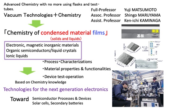
In Matsumoto Laboratory, under the catch copy of “Advanced chemistry with no more using test tubes and flasks”, we are engaged in studies on the vacuum deposition of condensed thin film materials, i.e. in solid and liquid, through a powerful combination of vacuum technologies and chemistry. Here, the thin films are defined as the materials whose thickness is less than 1 μm, sometimes can be down to the nanoscale, and they are one of the material categories that is most indispensable for the modern electronics industry. The materials that dealt with in our laboratory are widely ranged from inorganic electronic, magnetic, and superconducting materials to organic semiconductors, liquid crystals and ionic liquids, aiming to develop new processes and characterization tools, to explore new material properties and functionalities and to fabricate test devices with these film materials. We believe our originally developed elemental processes & characterization techniques and newly-discovered thin film materials will contribute to the real production industries as chemical knowledge-driven technologies for the next generation electronics which covers semiconductor devices, solar cells and secondary batteries.
Research Topics
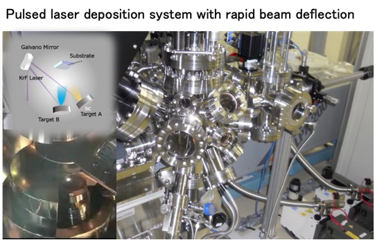
Pulsed laser deposition system with rapid beam deflection
For one example, we introduce a state-of-the-art thin-film vacuum deposition system that was originally developed in Matsumoto laboratory. As shown in the figure below, the apparatus consisting of silver-colored chambers of stainless steel, whose inside is in vacuum as high as it is in outer space, allows us the precision-controlled fabrication of thin films, excluding impurity inclusions as much as possible. That mechanical machine is called pulsed laser deposition (PLD). A UV-laser is introduced through a viewing port on the deposition chamber from the outside and rapidly scanned to almost simultaneously ablate solid material targets in the chamber, from which the gas source precursors come out are then deposited onto a substrate on the sample holder set at the side opposite to the position of the targets (Pls. see the video movie attached below). Accordingly, thin films with various compositions and structures can be fabricated by using the PLD machine [[Rev. Sci. Instrum.[90, 093901 (2019)]. For fabricating thin films of soft materials such as organic semiconductors, liquid crystals and ionic liquids, we have developed another laser deposition system similar to the PLD system, but one different point is the use of an infrared laser instead of the UV laser [Sci. Technol. Adv. Mater. 12 (2011) 054210].
Laser deposition of thin film materials
Here are some successful examples of thin films which were fabricated by means of such laser deposition methods as introduced in the previous section.
For the synthesis of inorganic ceramics materials, the process temperature often exceeds 1000℃ in conventional ceramics sintering processes, while the vacuum-PLD process enables to grow high-quality single crystalline films even at as low temperatures as below 1000℃. In the left-hand figure, a good example is the PLD growth of epitaxial self-assembled ferro(i)magnetic spinel (CoFe2O4 (CFO)) and ferroelectric bismuth layered perovskite (Bi5Ti3FeO15 (BTFO)) pillar-matrix nanostructure films. This is a new intriguing thin film material because a careful tuning of the interfacial strain between these two-phase materials leads to emergence of a new ferroelectric phase and an arbitrary switching of polarization phenomenon[ACS Nano 7, 11079 (2013), Nat. Commun. 5, 4971 (2014) ].
As for the thin film synthesis of organic semiconductors, liquid crystals and ionic liquids by using the infrared laser deposition, the structures and films of ionic liquids termed as “nano-ionic liquids”, whose size and thickness are on the order of nanometer scale, have been successfully obtained, as shown in the right-hand figure, and their properties such as ionic conductivity are under investigation[ACS Nano 4, 5946 (2010), ACS Nano 12, 10509 (2018)].
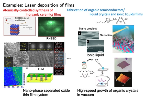
Furthermore, we have proposed for the first time a new process of “ionic liquid-assisted vacuum deposition”, where the deposition is made via such nano- and micro-scale ionic liquids that have been pre-prepared on a substrate[Cryst. Growth Des. 10, 3608 (2010)], and successfully demonstrated a rapid growth of organic single crystals such as pentacene [Cryst. Growth Des. 11, 2273 (2011)]. More recently, it has been found that this infrared laser deposition method is also powerful to the thin film fabrication of metal hydrides such as LiBH4[ACS Appl. Electron. Mater., 1, 1792 (2019)].
Development of new characterization tools compatible to the vacuum processes
In Matsumoto laboratory, we challenge to develop, besides new vacuum deposition processes, new characterization tools compatible to the vacuum processes. The left-hand figure displays a laser microscope system that was specially designed in Matsumoto laboratory to observe high-temperature solution growth interfaces. As the first demonstration in the world, the image shows a snapshot of the solution growth interface of a SiC crystal layer, where the step-flow behavior is clearly observable on the growing crystal surface (Pls. see the video movie attached below)[Cryst. Growth Des. 17, 2844 (2017)].
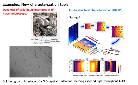
As shown in the right-hand figure, we also have established a new high-throughput approach with a grazing incidence X-ray diffraction technique (@Spring-8) for structural characterizations of organic thin film libraries, on which its doping level and growth temperature are continuously varied along the X- and Y- axis, respectively on a single substrate. Combining with a machine-learning program and thereby much reducing the number of the mapping data points over the library, we have come to be able to much more efficiently characterize organic thin films and the crystallinity was reconfirmed to significantly depend on the doping level and growth temperature[ACS Comb. Sci. 22, 348 (2020)].
Furthermore, we have developed a new in situ PLD system that is combined with an electrochemical cell, aiming to explore a new semiconductor electrochemistry. In this system, epitaxial oxide thin film electrodes which are prepared by using PLD can be subjected to electrochemical measurements with ionic liquid in a vacuum without exposing the sample to the air[ChemElectroChem 2020, 7, 3253-3259].
New material properties and device functionalities
Finally, are introduced in this section some of new material properties and device functionalities that have been explored and investigated so far.
The first topic is the development of a new vapor deposition process for high-quality SiC single crystal films SiC, which development we had been working on under the funding support of JST-ALCA until 2018. In this project, we employed a vapor-liquid-solid (VLS) mechanism. This process is rather close to the solution growth process than the vapor deposition in that the deposition is made via a high-temperature melt flux (over 1000℃), which is often used in the corresponding solution growth. As a result, we succeeded in the fabrication of high-quality SiC single crystal films as comparable to the bulk single crystals, as reinforced by the observation of good rectifying I-V characteristics in their Schottky junctions[Materials Today Chemistry 16 (2020) 100266].
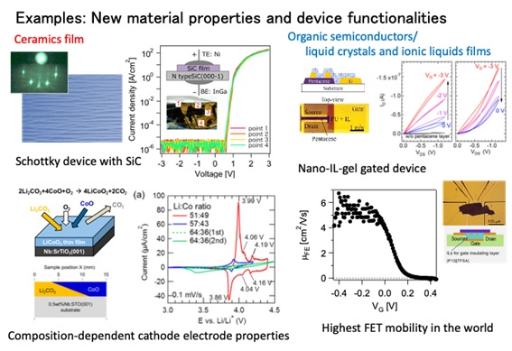
The second is to grow LiCoO2 epitaxial thin films, which material is well known for its good performance as a cathode electrode in Li ion batteries. For this, from the viewpoint of precision controlling the composition ratio of Li/Co, we attempted to “synthesize” a LiCoO2 film on a substrate by PLD through the following chemical route:
2Li2CO3 + 4CoO + O2 → 4LiCoO2 + 2CO2↑
, which is a model reaction scheme that is often used in the ceramics sintering processes for bulk LiCoO2. By a high-throughput approach of lateral composition gradient and 2D-XRD mapping techniques that are often used in a thin film-combinatorial science, the crystallinity and surface morphologies of the compositionally optimized LiCoO2 films have been much improved, thereby exhibiting higher battery performance[ACS Comb. Sci. 18, 343 (2016)].
The third is to develop organic field effect transistors (OFETs). We have demonstrated the highest performance of ionic liquid-gated FET (so called electric double layer transistor: EDLT) with the pentacene single crystals synthesized through ionic liquid-assisted vacuum deposition, which has been explained in the previous section. Furthermore, we have succeeded in one-pot vacuum synthesis of new nanogels constituted of polyurea filled with an ionic liquid, the nanogels whose thickness can decrease down to the nanoscale. This ionic liquid nanogel sheets are confirmed to work a gate electrolyte instead of bulk ionic liquid in EDLTs, opening the way for the development of a future “electrochemical device integration” technology[ACS Appl. Nano Mater. 2020, 3, 9610-9615].
Designed by CSS.Design Sample