Molecular Materials Design, Department of Applied Chemistry, School of Engineering, Tohoku University
Facilities and Equipment

Vacuum chamber systems
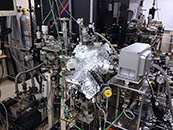 |
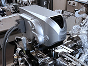
In situ Combi-PLD-Confocal Laser Scanning Microscope System PLD-grown films with different compositions and structures can be integrated on a single substrate in one experiment, and the confocal laser scanning microscope which is directly attached to the PLD allows direct observation of local surface areas on the sample without being exposed to air, which maximum temperature in observation is as high as 1800℃. |
 |
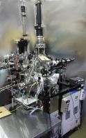
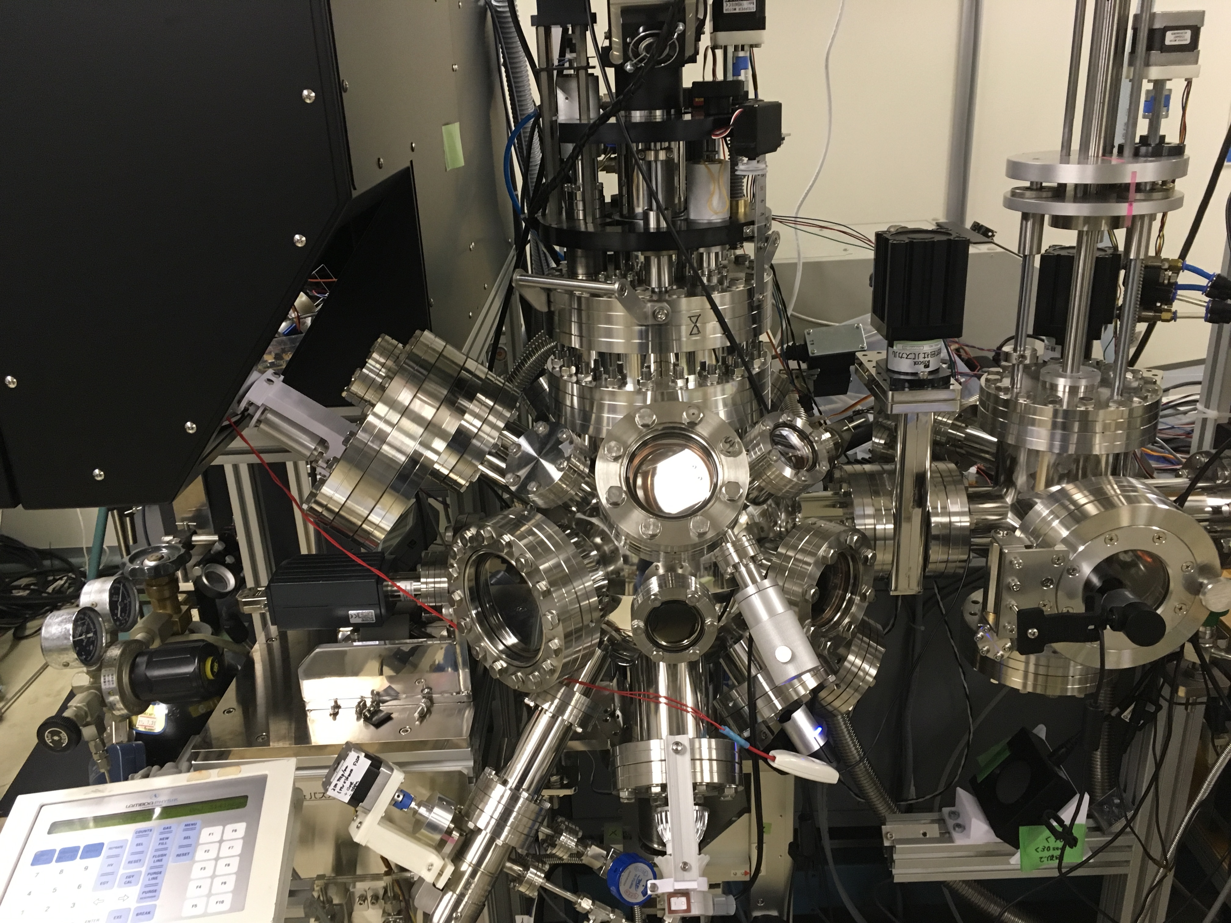
Ultra-High Temperature PLD System Ceramics films can be grown by PLD at high temperature over 1000℃ with high growth rate, e.g., 30μm/h in thickness. |
 |
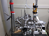
In situ PLD-STM System PLD-grown film surfaces are in situ characterized by LEED/AES and by STM with atomic resolution. |
 |
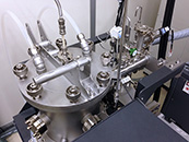
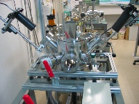
In situ Electrochemical-PLD System PLD-grown films can be electrochemically characterized by in situ approach in vacuum with ionic liquid used as electrolyte. |
 |
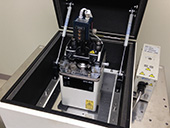
Compact IR Laser Deposition System A revolver type sample holder unit enables to set multiple samples in the vacuum chamber and to successively deposit soft materials on each substrate in one run experiment. In the deposition and substrate heating, IR lasers are used, respectively. The precision control of the substrate temperature is possible around at 100-300 ℃ within the error of ±0.1℃ by directly attaching a thermocouple to the sample, combined with the IR laser heating device. |
 |
Double IR laser Deposition System Two different soft materials can be simultaneously deposited by using two independent IR lasers. In situ optical scale observation of the growth process is available through a long-distance focusing optical microscope. |
 |
PLD with Rapid Beam Deflection System Rapid laser scan enables to ablate two different target materials with almost no time delay between the ablations, and to deposit, e.g., compositionally-graded films according to a computer-programmed laser pulse sequence of the two target materials during deposition. |
Evaluation equipment
 |
X-Ray Diffraction (XRD) XRD is used to examine the crystal structure and thickness of film materials. In this system, the X-ray beam which is focused to a spot size of 100 μm, can be scanned over the surface to map out the spatially dependent crystal structures of the film. |
 |
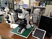
Confocal Laser Scanning Microscope (CLSM) The surface morphology and its height profiles of films are observed by means of a CLSM. |
 |
Atomic Force Microscopy (AFM) AFM is used to observe surface morphologies of not only solid, but also liquid thin film materials on a nanometer scale. |
 |
Differential Interference Contrast (DIC) Microscopy DIC, which is among optical microscopes, enables to observe very small height differences on the surface of thin film and bulk materials. |
 |
Stylus Surface Profiler This apparatus is for measurement of film thickness by scanning a stylus loaded into contact with the surface. |
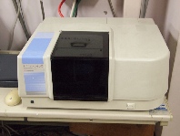 |
Fourier Transform Infrared (FT-IR) Spectroscopy FT-IR is used to identify the types and nature of chemical bonds in solids and molecules. |
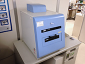 |
X‐Ray Fluorescence (XRF) analysis XRF analysis is used to determine the chemical composition of thin film and bulk materials. In this system, the X-ray beam which is focused to a spot size of 50 μm, can be scanned over the surface to map out the spatially dependent composition of the material. |
Other
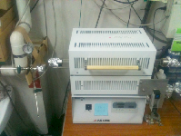 |
Tube Furnace with Gas Flow Control Tube furnace is used for preparation of substrates, if needed, under gas flow conditions. |
 |
Plasma Cleaner Plasma cleaner is used for cleaning substrates. |
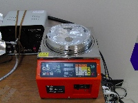 |
Spin Coater Spin Coater is used for the wet-process to coat thick films. |
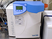 |
Ultra-Pure Water Machine Ultra-pure water is used for washing substrates and for electrochemical experiments with water-based electrolytes. |
Designed by CSS.Design Sample