![]()
I. Surface Structure
In order to understand interface structure an effort is being made to establish
methods to form well-defined solid/liquid interfaces. This is being done by
using many types of single-crystal surfaces along with both aqueous and nonaqueous
solvents. Research is also focusing on new ways to make measurements and to
control surfaces using in situ scanning probe microscopes, such as STM and AFM.
In addition, the use of ultrahigh-vacuum surface-analysis techniques is being
pursued. As part of this pursuit, special multi-chamber vacuum systems are being
developed in which solid samples can be removed from a liquid and then analyzed
without experiencing oxidation or contamination.
II. Surface Formation
Regarding interface formation, work is concentrating on the bond-formation reactions
which occur at the solid/liquid interface. For example, the mechanisms by which
metal and semiconductor surfaces are electrochemically formed and dissolved,
thin-film crystal growth processes, as well as the adsorption and orientation
of ions and molecules are being pursued. In addition, the formation of modified
surfaces and new methods for making thin films using knowledge gained about
reactions at the solid/liquid interface is being studied.
III. Surface Fabrication
Another area of concentration concerns interface fabrication, while concentrating
on reactions that break bonds at the solid/liquid interface. The processes involved
in chemical and electrochemical etching as well as in dissolving adsorbed molecular
layers should hopefully be clarified. To this end, the electrochemical energy
and optical energy necessary to control reactions at the solid/liquid interface
are being applied. A search for technology to control metal and semiconductor
surfaces at the atomic and molecular levels is also being conducted.
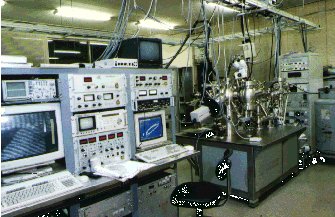
Application of UHV-EC to Analysis of Adlayers from Anions
We constructed two UHV-EC apparatus that are designed to process electrode surfaces
in electrochemical environment and to transfer them into ultrahigh vacuum environment
for examination by STM, LEED, AES, etc. which cannot be done in liquid phase.
Figure 1 shows one of our UHV-EC machines. Combination
of surface analysis tools in UHV and electrochemical STM led to high precision
determination of adlattice structures of halogens and cyanide ions on gold and
silver electrodes. Figure 2 shows continuous
structure variation of iodine on Au(111) under potential control. In this figure,
the LEED patterns correspond to the "reciprocal space image" of the
in-situ STM images. The LEED patterns were utilized to determine lattice constants
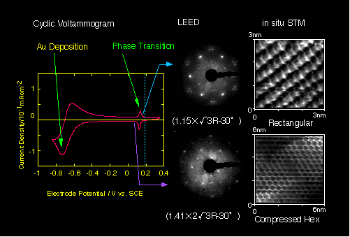
of iodine adlayer. Figure 3 shows a voltage-current
curve, in-situ STM images and corresponding LEED patterns of gold-cyanide surface
complex compound on Au(111).
Formation of Highly-ordered Monolayers of Organic Molecules
on Electrode Surfaces
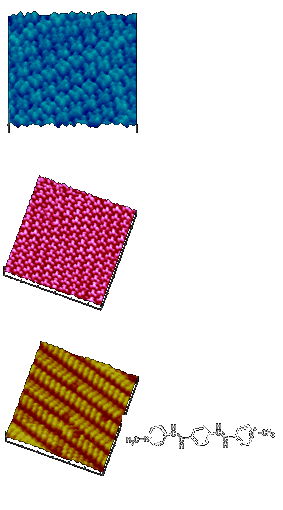
Our finding by in situ STM is that porphilins, crystal violet and other aromatic
planer molecules form highly-ordered monolayers upon mobilization by iodine-passivated
gold electrodes. The STM images resolve these organic molecules in detail. By
this approach, many kinds of organic molecules and substrates have been tested.
Figure 4 shows self-organized adlayers of porphyrin,
crystal violet and PPV.
Formation of Chemisorptive Adlayers of Organic Molecules
and Ions on Electrode Surfaces
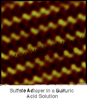
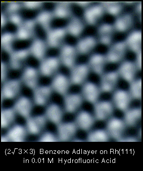
In situ STM investigations revealed sell-ordered sulfate anions, cyanide anions,
etc. on platinum and rhodium electrodes which exhibit relatively strong chemisorptivity.
We found for the first time that water molecules and cations can be incorporated
into these adlayers. (Figure 5) In situ STM also
resolved internal structures of adsorbed benzene, quinones and other delivertives
with high resolution (Figure 6).
Atomic-scale Observation of Semiconductor Electrodes
and their Etching Processes
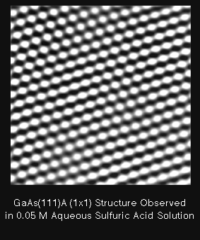
We successfully observed hydrogen-terminated surfaces of silicon and gallium
arsenide single-crystalline electrodes in aqueous solutions (Figure
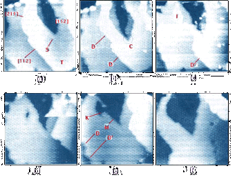
7). Furthermore, dynamic atomic-scale observations of these semiconductor
surfaces during etching processes (Figure 8),
which might lead to foundation of the basis of atomically flat substrate surfaces
demanded in semiconductor industry of the next generation.
Observation of the Structures and Formation Processes
of Electrodeposited Metals
The processes of formation of thin films of gold and silver were surveyed by
in situ STM atomic resolution. Silver deposition on gold single-crystalline
surfaces, in particular, the adlattice structures of Ag formed by underpotential
deposition (UPD) depend on the composition of liquid phase. The multilayer deposit
of Ag on the same surface is a high quality single-crystalline film. Figure
9 shows an in-situ STM image of the (4x4) structure of Ag on Au(111) formed
by underpotential deposition in a perchlorate solution.
Preparation and Observation of Clean Surfaces of Base
Metals
We devised methods of cleaning single-crystalline surfaces of the base metals
such as nickel, cobalt, zinc, etc which were believed difficult to prepare .
For the first time we observed the surfaces in action in acidic solutions by
in situ STM. Furthermore, we observed the process of passivation of these surfaces
by oxidation and the process of etching of atomically flat surfaces by presence
of sulfur adatoms. Figure 10
shows time-sequential STM images of S/Ni(100) that exhibits catalytic atomic
etching.
Observation of Adlayers on Electrodes in Non-aqueous
Electrolytic Solutions
Attempts were made to purify polar non-aqueous solvents such as propylene carbonate
and acetonitrile and to observe adsorption of iodine on gold and platinum electrodes
by cyclic voltammogram and in situ STM. A different series of adlattice structures
of iodine was found in propylene carbonate solutions by in situ STM. Figure
11 shows an image out of that series. This successful study opens an unprecedented
approach of introducing a variety of non-aqueous solvents into nano-electrochemistry
at the electrode surface.