Quantum Physical Chemistry
Development of innovative radiation sensors having the best quality in the world
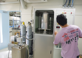
We are exploring a new frontier in materials chemistry from the viewpoint of ultrafast dynamics, peculiar electronic excitation generated by ionizing radiations, and nanostructures. At the moment, we are mainly focusing on the development of novel scintillation materials, which can be used to manufacture radiation sensors. Our aim is to develop excellent scintillation materials in order to manufacture a novel high-quality detector that can very accurately determine arrival time of ionizing radiation, i.e., a detector with a very high time resolution. We have already developed a detector that exhibits a time resolution of less than 100 ps (= 10 billionth of a second), which in the best time resolution reported so far.. Our unique approach allow the production of novel high-quality scintillation materials.
Control ling the electronic states is very important in the development of scintillation materials, because the scintillation process is dependent on the nature of the electronic states. We have been employing nanotechnology to achieve this control. One example is the development of organic-inorganic perovskite-type compounds, in which a two-dimensional structure (quantum well) is naturally formed. We have succeeded in developing novel high-quality scintillation materials, and these materials have attracted much attention from researchers and potential users. This was the first successful development of scintillation materials by utilizing the quantum confinement effect. At present, by using various fabrication methods, we are developing novel materials of higher quality for practical use. These high-quality materials will greatly contribute to advances in basic science and industrial applicationsy.
We are investing considerable efforts to develop materials having the best quality in the world. In the course of our daily research activities, we often encounter unprecedented results. This is a major source of inspiration that motivates us to conduct further studies and has helped us carry out pioneering research in this unexplored field of science. The vast universe of science can benefit from our diligence and enthusiasm.
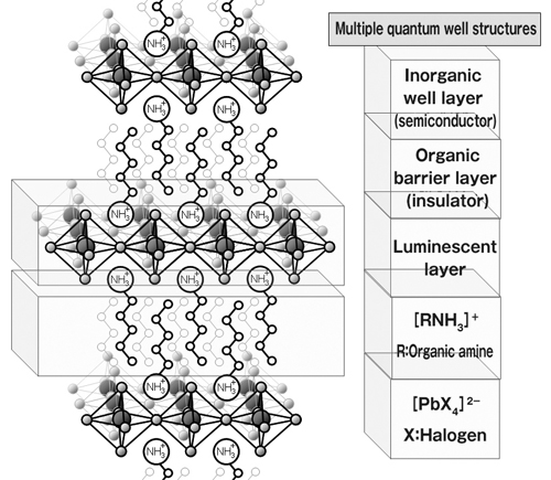
Schematic structure of a novel scintillation material: organic-inorganic perovskite-type compounds
Main Research Themes
- Fabrication of ultrafast scintillation materials (light-emitting radiation sensors) by using nano-technology
- Development of novel radiation sensors using correlated electrons system
- Structural analysis of minute space within materials using elementary particles- from atomic vacancies to pores at nanometer scale
- Synthesis of self-organized semiconductor nanostructure to achieve novel optical and magneto-optical properties
Professor of Applied Chemistry
Doctor of Engineering
Keisuke Asai
Graduated from Asahigaoka High School (Aichi Prefecture) in 1981. Graduated in 1986 from the Department of Applied Physics, Faculty of Engineering, University of Tokyo, majoring in physics engineering, before joining Sony. Completed a master's course at the University of Tokyo Graduate School of Engineering in 1991 and was appointed as an assistant at the University of Tokyo Graduate School of Engineering that year. Served as a lecturer before being appointed assistant professor at the University of Tokyo Graduate School of Engineering in 1999. Assumed current position in 2003. "I was fascinated by things like stars, rocks and insects from an early age, particularly fossils, which inspired in me a sense of the drama of ancient history." The slogan of the Asai Laboratory is: Don't be too serious, but do be diligent.